Researchers from the University of Strasbourg and CNRS (France), in collaboration with TU Dresden (Germany), have developed a production method of high-quality violet phosphorous for applications in (opto)electronics. These results have been published in the Journal of the American Chemical Society.
Two-dimensional (2D) materials have attracted much attention due to their fascinating electrical and optical properties, enabling a wide range of high-performance applications in nanoelectronics, optoelectronics, spintronics, etc. Importantly, the vast majority of 2D semiconductors can conduct electrons (n-type behavior) or both electrons and holes (ambipolar behavior), whereas only a few 2D semiconductors capable of conducting holes (p-type behavior) have been identified so far. Therefore, it is crucial to discover new p-type 2D semiconductors to boost the advance of 2D materials for next-generation complementary (opto)electronic technologies.
Violet phosphorus (VP) – a stable form of phosphorous – has recently emerged as the most promising candidate as the next game changer in the family of 2D semiconductors, largely due to its unique band structure as well as higher stability than black phosphorus. Nevertheless, the production of high-quality VP sheets remains challenging, hindering the exploration and exploitation of their full potential in 2D (opto)electronics.
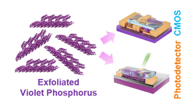
In this work, the researchers from Strasbourg and Dresden have developed a reliable and scalable synthetic strategy to produce high-quality few-layer-thick VP flakes, allowing the first investigation of their electrical and optical properties. After growing centimeter-scale VP crystals, mild liquid-phase sonication was used to “peel off” VP nanosheets featuring high structural integrity, large lateral dimensions (up to 2 μm), and low thicknesses (down to the monolayer limit).
Thanks to the p-type conduction and superior hole mobilities of the exfoliated VP flakes, different thin-film devices, such as field-effect transistors, photodetectors, and complementary metal oxide semiconductor (CMOS) logic circuits, with excellent electrical and optical performances could be fabricated. These results demonstrate the huge potential of VP for the future development of energy-efficient large-area (opto)electronic technologies.
Two-Dimensional Violet Phosphorus: A p-Type Semiconductor for (Opto)electronics
Antonio Gaetano Ricciardulli, Ye Wang, Sheng Yang, and Paolo Samorì*
J. Am. Chem. Soc., 2022, 144, 3660–3666 (DOI: 10.1021/jacs.1c12931)