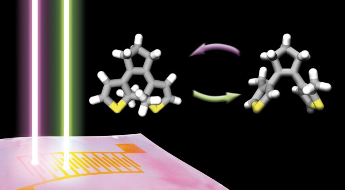
Researchers from the University of Strasbourg & CNRS (France), in collaboration with the Humboldt University of Berlin (Germany) and the University of Nova Gorica (Slovenia), have shown that a carefully chosen blend of a small photoswitchable molecule and a semiconducting polymer can be used to fabricate high-performance memory devices that can be written and erased by light. Such multilevel (8-bit!) optical memories have also been implemented on flexible substrates, paving the way to applications in wearable electronics, E-papers, and smart devices. These results have been published in Nature Nanotechnology.
In the quest to improve the data storage capability of everyday electronic devices (random-access memories, hard disk drives, USB flash drives, etc.), alternative strategies to conventional silicon-based technologies need to be developed. The continuous miniaturization of electronic circuits, leading to the integration of a larger number of memory cells per unit area, has already shown its limitations due to the increased fabrication complexity. Another appealing approach consists in developing memory elements capable of storing not just one but multiple bits of information per device, commonly refered to as multilevel memories.
Now a European team of researchers from Strasbourg, Berlin, and Nova Gorica developed a light-responsive organic thin-film transistor by blending a custom-designed molecule serving as miniaturized optical switch with a high-performance semiconducting polymer. Upon illumination with ultraviolet and green light to “write” and “erase” information, respectively, the molecular switch undergoes a reversible interconversion between two distinct forms, one enabling and the other one preventing current to flow through the surrounding semiconducting polymer.
By integrating these components into transistor devices and using short laser pulses the researchers were able to construct multilevel memories with a data storage capacity of 8 bits. Importantly, their prototype devices combine high endurance over 70 write–erase cycles and data retention times over 500 days.
Taking the work yet to another level, the team could transfer the device concept to flexible and light-weight polymer substrates, such as polyethylene terephthalate, to replace the commonly used rigid silicon. The resulting “soft” architecture preserves its electrical characteristics after 1000 bending cycles, thereby demonstrating its robustness and suitability for flexible electronics.
These findings are of great importance for the realization of high-performance smart and foldable electronic (nano)devices programmed by light with potential applications in flexible, multilevel high-density optical memories, logic circuits, and more generally in the next generation optoelectronics.
Reference:
“Flexible non-volatile optical memory thin-film transistor device with over 256 distinct levels based on an organic bicomponent blend”
Tim Leydecker, Martin Herder, Egon Pavlica, Gvido Bratina, Stefan Hecht*, Emanuele Orgiu* and Paolo Samorì*
Nature Nanotechnology (2016), DOI: 10.1038/nnano.2016.87

